In this section we demonstrate the key capabilities of the UPD technology as an additive manufacturing method for microfabrication. By this selection of examples, we want to demonstrate the versality of the UPD approach, in terms of the material to be printed (metallic pastes, insulating inks), shape of the printed structures, as well as type and shape of the substrate (including substrates with pre-existing features, i.e., steps).
Conductive meshes: gold, silver, and copper
Conductive meshes are a vital part of rigid and flexible displays, as well as e-paper, transparent displays, and smart devices. However, the choice of the conductive material depends on various design constraints, cost analysis, specific architecture, and compatibility with other components of the device. In this section we will present conductive meshes printed using pastes based on silver, copper, and gold nanoparticles. In Fig. 11a we demonstrate a conductive mesh with 5 μm wide lines printed using paste based on silver nanoparticles (85 wt% of solid content). The whole sample is shown in the inset; in Fig. 11b we show a conductive mesh printed using copper paste (80 wt% of solid content). In this design the lines have various widths: 7 μm in the horizontal direction and 15 μm in the vertical direction. The inset shows lower magnification of the sample. In Fig. 11c we present a conductive mesh printed using gold paste (80 wt% of solid content). In the inset we show a heat map corresponding to the height profile. Finally, in Fig. 11d we demonstrate conductive mesh printed on glass/IZO substrate using paste based on silver nanoparticles (85 wt% of solid content). The line width is 5.5 μm (horizontal direction) with pitch of 105 μm and 18 μm (vertical direction) with pitch of 315 μm. Such design results from a trade-off between the optical and electrical properties of the film. The mesh was sintered in 250 °C for 10 min. It allowed us to achieve sheet resistance of 1.5 Ω/□ with the transparency of 90%. Commonly used transparent conductive films (TCFs) based on indium tin oxide (ITO) are characterized by sheet resistance in the range 10–25 Ω/□ with transparency > 90%. Therefore, TCF prepared using the UPD approach gives significantly lower sheet resistance with similar transparency. Compared to TCFs prepared using other additive manufacturing techniques, transparent electrodes can be prepared using EHD printing, achieving sheet resistance of 3 Ω/□ and transparency of 96%27. For TCFs printed using Inkjet, one obtains lower transparency due to limited resolution of the printing process, e.g., sheet resistance of 13 Ω/□ with transparency of 81.9%; we note, however, low sintering temperature of 60 °C28.
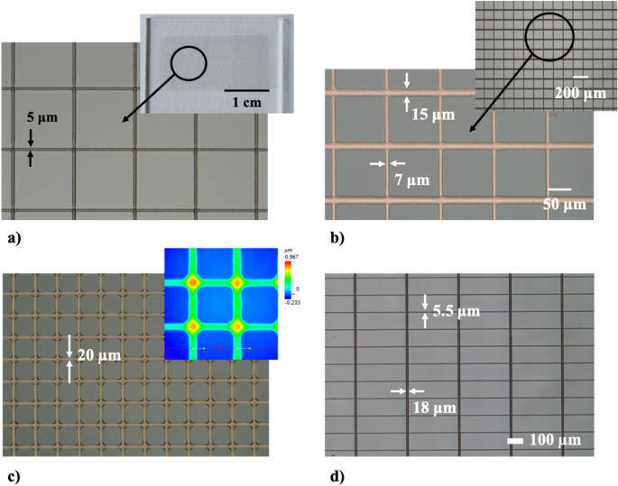
Example conductive meshes printed using highly-concentrated pastes. (a) Conductive mesh with 5 μm wide lines, printed using paste based on silver nanoparticles (85 wt% of solid content). The whole sample is shown in the inset; (b) conductive mesh printed using copper paste (80 wt% of solid content). The line width is 7 μm (horizontal direction) and 15 μm (vertical direction). The inset shows distant view of the sample; (c) conductive mesh printed using gold paste (80 wt% of solid content). In the inset we show a heat map corresponding to the height profile; (d) conductive mesh printed on glass/IZO substrate using paste based on silver nanoparticles (85 wt% of solid content). The line width is 5.5 μm (horizontal direction) and 18 μm (vertical direction).
Printing on steps
UPD gives the possibility to print 3D interconnections for advanced packaging, including hybrid electronics (combining printed electronics and silicon technologies)1,29. In this regard, in Fig. 12 we demonstrate the capabilities of the UPD technology to print on steps with various heights. Figure 12a demonstrates repeatable and continuous silver lines with a width of 15 µm printed on the step with the height of 150 µm. Therefore, the step height is ten times the width of the lines. Figure 12b shows a 10 µm wide silver line printed on a microchip with the height of 350 µm. The range of the line widths, as well as the range of the step heights demonstrated in the above examples fully satisfies the requirements for the fabrication of interconnects in modern microelectronic devices, such as µLED arrays.
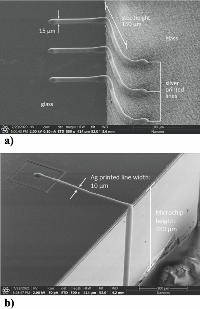
(a) Repeatable and continuous silver lines with a width of 15 µm printed on the step with the height of 150 µm, (b) 10 µm wide silver line printed on a microchip with the height of 350 µm.
Microdot deposition
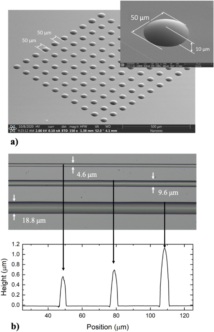
Another capability of the UPD method is the possibility to print microdots. Microdots made from a conductive material can be used for making electrical contacts. In Fig. 13a we show microdots printed using the UPD approach (the bar corresponds to 100 μm), whereas in Fig. 13b we demonstrate higher magnification of the sample (the bar denotes 20 μm). In the inset of Fig. 13b there is a cross section of the dots profile obtained using a profilometer. The dots have the diameter of around 8 µm and the height of around 800 nm. One can also notice a smooth, lens-like shape of the microdots, which is desired, e.g., in the case of deposition of additional layers. Such a shape significantly reduces the risk of cracks in the subsequent layers. This is very different from microdots obtained using lithography, which generally have a rectangular shape. Finally, Fig. 13c we show an example of high-resolution picture consisting of microdots printed using the UPD approach.
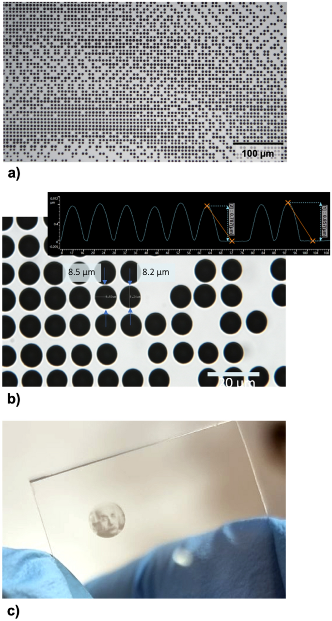
(a) Microdots printed using the UPD approach, the bar denotes 100 μm; (b) higher magnification of the sample, the bar denotes 20 μm and the inset shows cross section of the dots profile obtained using a profilometer; (c) an example of high-resolution picture consisting of microdots printed using the UPD approach.
The key advantages of using the UPD method to print microdots are: (1) high resolution, diameter below 10 µm; (2) high repeatability and printing stability; (3) high aspect ratio (800 nm height to 8 µm diameter); (4) the ability to cover large areas. These results also demonstrate the ability to deposit a precisely defined amount of material.
Deposition of insulating materials
Up to now we have discussed printing using high-viscosity conductive materials developed in-house. In this section we focus on insulating materials obtained from external suppliers. In Fig. 14a we show an array of microdots printed with photoresist AR-P 3110 (obtained from: Allresist GmbH). This material is characterized by the viscosity of 12 cP, therefore orders of magnitude lower than in the case of the conductive pastes. The distance between the printed dots is equal to 50 μm, the dot diameter is equal to 13 μm, and the dot height is equal to 10 μm. The microdots are characterized by parabolic shape, which may, for example, simplifying the deposition of subsequent layers without the risk of cracks.
(a) Array of microdots printed with photoresist AR P 3110, characterized by the viscosity of 12 cP; (b) Set of lines printed using SU-8 photoresist together with the height profiles.
As another example, in Fig. 14b we show a set of lines printed using SU-8 photoresist provided by Sigma-Aldrich. Below the image of the lines there are the height profiles. We demonstrate lines with the width raging from 4.6 μm to nearly 19 μm. As in the previous examples, the line width depends on the nozzle opening, printing speed, and applied pressure.
Open-defect repair in OLED arrays
Displays based on organic light-emitting diodes (OLEDs) have significant advantages over other display technologies14,15,16. This includes superior image quality and lower power consumption. Yet, to achieve a dominant position in the market, OLED displays require manufacturing technologies that offer high throughput, precision, and low cost at the same time. Yield management is one of the biggest challenges and it strongly affects the overall costs. In this regard, the ability to repair open defects is in high demand for OLED manufacturers17.
Open defects are defined as a local lack of conductive material in an OLED TFT array. Such defects may appear at the production stage and usually result in the product rejection. The problem is becoming even more significant in the case of large-area displays and ongoing miniaturization of display components with the aim of increasing the display resolution.
Current repair methods include30,31,32,33,34: Electrohydrodynamic (EHD) printing, Laser Chemical Vapour Deposition (LCVD), and Laser-Induced Forward Transfer (LIFT). The main disadvantages of these technologies are limited throughput and cost. Moreover, EHD can damage active electronic systems in integrated circuits (due to electrostatic discharge defects); LCVD, and LIFT provide only a limited possibility to obtain paths with a width below 10 µm, and LCVD uses toxic gases. For microdispenser technique for disconnection repair12, printing lines with the line width below 10 µm is only possible with a mask film.
An OLED display array is a complex substrate, both regarding the topography and composition of the materials. To repair a defect, it is necessary to properly position the printing nozzle and ensure that the printed connection is uniform and continuous, regardless of the shape of the substrate and its wetting properties.
Finally, the UPD features presented so far allow to demonstrate an electrical connection printed on a real OLED substrate. In Fig. 15a we show a silver line with a width of 1 µm and length of 20 µm printed on an OLED substrate, whereas in Fig. 15b we demonstrate a cross section of the line. Platinum layer is for imaging purposes.
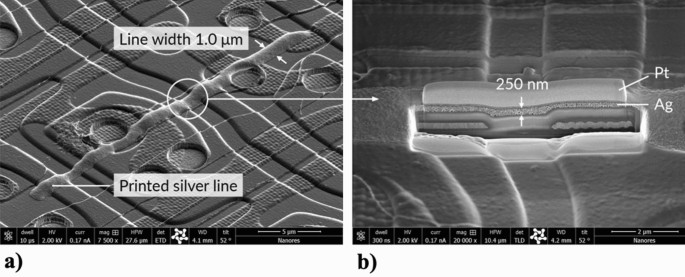
(a) Silver line with a width of 1 µm and length of 20 µm printed on an OLED substrate; (b) cross section of the line. Platinum layer is for imaging purposes.
Array of source/drain structures for printed flat panel display
In Fig. 16 we demonstrate the capabilities of the UPD technology for mass production. The figure shows part of the sample of 7500 printed segments for transistors with the line width of 4 μm. The key feature of UPD in this case is not only the line width, but also the ability to reduce the interline distance to single micrometers. Moreover, the shape to be printed can be defined arbitrarily, which supports lean manufacturing.
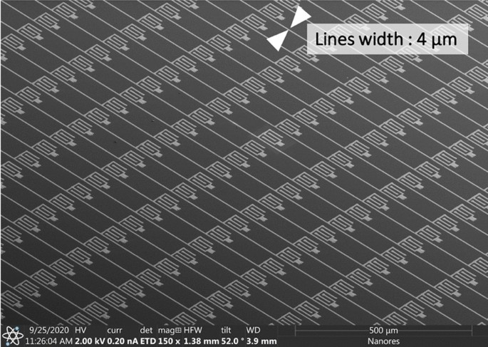
Demonstration of the capabilities of the UPD technology for mass production. The figure shows 7500 printed segments for a thin-film transistor array with the line width of 4 μm. The key feature of UPD in this case is not only the line width, but also the ability to reduce the interline distance to single micrometers and below.
LED matrix powered using printed silver lines
As a final case, we give an example of a 2 × 2 matrix consisting of Surface Mounted Device (SMD) LEDs and powered using printed silver lines made from CL85 paste. The sample was fabricated as follows: First, we printed two horizontal conductive tracks. Then, we deposited four segments of insulating material (polyimide ink with the viscosity of 4000 cP) where the horizontal and vertical conductive tracks were planned to intersect to avoid short circuit. Finally, we deposited vertical conductive tracks and pads for SMD LEDs. In this case, we used the UPD approach to deposit both conductive and insulting materials. The resulting matrix size is 5 × 5 cm and the line width is around 16 µm. In Fig. 17 we show lighting up of the diodes one by one.
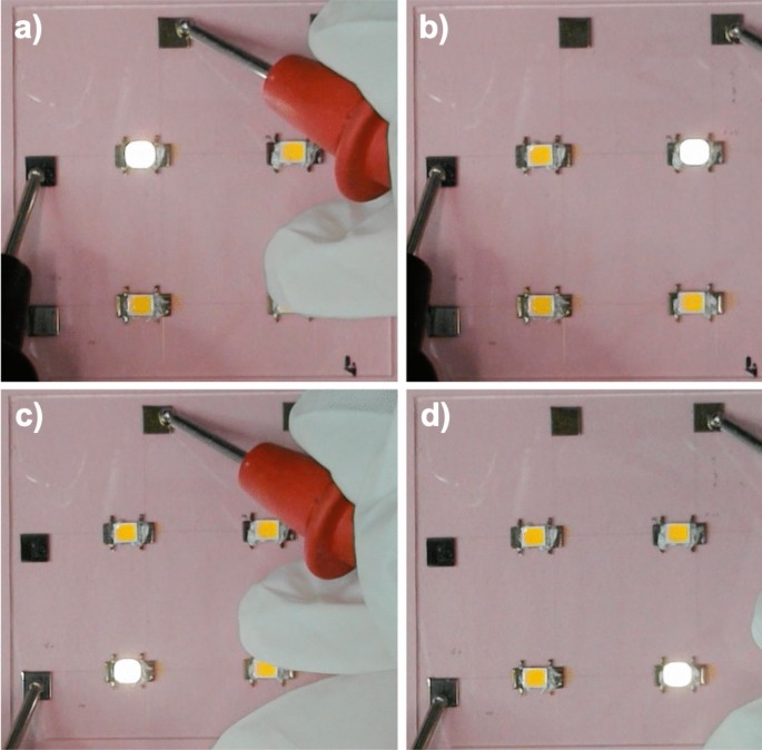
2 × 2 matrix consisting of Surface Mounted Device (SMD) LEDs and powered using printed silver lines made from CL85 paste. The matrix size is 5 × 5 cm and the line width is around 16 µm. Mounting the LEDs and measurements: courtesy of dr. Selen Solak from Humboldt-Univeristät.
Durability of the printed structures
Durability and long-term stability of the fabricated structures are important factors for industrial applications. In this section we discuss an impact of various external parameters on the printed structures: long-term stability, adhesion of the printed structures to the substrate, resistance to high temperatures, multiple folding, impact of humidity, and UV exposure.
For long-term stability, the relative increase of electrical resistance of silver lines with the width of 10 µm after two weeks is around 6.5%. The samples were kept in vacuum, but we used no other protection, like passivation/encapsulation layer. In practical cases, the printed structures would be embedded in microelectronic systems with much higher level of protection. Therefore, we would assume that the relative resistance increase of 6.5% in two weeks after printing is the worst-case scenario.
To test the adhesion of the printed structures, we prepared a number of samples and measured the resistivity before the adhesion test, after a single Scotch-tape test, and after ten Scotch-tape tests. The relative increase of electrical resistance for 5 µm wide silver lines after performing standard 10 × Scotch test is between 4 to 7%. The results are shown in Fig. 18a.
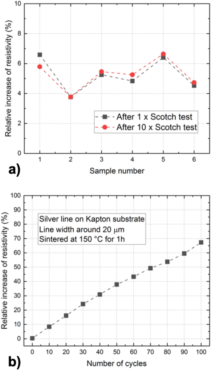
(a) Adhesion test of the printed structures: relative increase of resistivity for 5 µm wide silver line after performing 1 × Scotch-tape test and 10 × Scotch-tape test. (b) Multiple folding test: relative increase of resistivity as a function of the number of folding cycles.
We also performed multiple folding tests of silver lines printed on Kapton substrate, up to 100 bending cycles. The line width is in the range from 21 to 23 µm, and the structures were sintered at 150 °C. The results are shown in Fig. 18b.
When it comes to the impact of high temperature on the printed structures, the practical limitation is the substrate. Besides photonic sintering, we use thermal sintering to sinter the printed structures. The highest temperature we achieved during the thermal sintering of the structures printed on glass is 350 °C (e.g., lines with the width of 5 µm were placed in the oven for 10 min at 350 °C). The printed structures not only survived such high temperature, but we also achieved the best electrical conductivity. However, in the case of structures printed on a PET foil, the maximum sintering temperature is 120 °C35, which is the limitation related to the substrate. For PEN foil, the maximum temperature we used was 269 °C.
Humidity may be detrimental to the printed structures. However, printed conductive structures are usually protected from environmental factors by coatings and encapsulation36,37. Using the UPD method and the materials discussed above, one can coat printed metallic structures with SU8, deposited using the same printing system.
Finally, regarding UV exposure, we use UV lamp to harden SU8 (wavelength is 365 nm, maximal irradiance is 500 µW/cm2) and in many cases printed metallic structures are exposed to UV light as well. E.g., part of the printed line is covered with SU8, so that we can print another line on top, perpendicular to the first one, to achieve an intersection and avoid short-circuit. For the parameters of the UV light mentioned above, we have not observed any detrimental effect of UV light on the printed structures.